PCB Layout
The ESP32-S3-DevKitC-1 is a two-layer PCB designed for manufacturing simplicity while maintaining good RF performance.
Board Dimensions
| Parameter | Value |
|---|---|
| Length | 62.74 mm |
| Width | 25.40 mm (at module) |
| Thickness | 1.6 mm (standard) |
| Header Pitch | 2.54 mm |
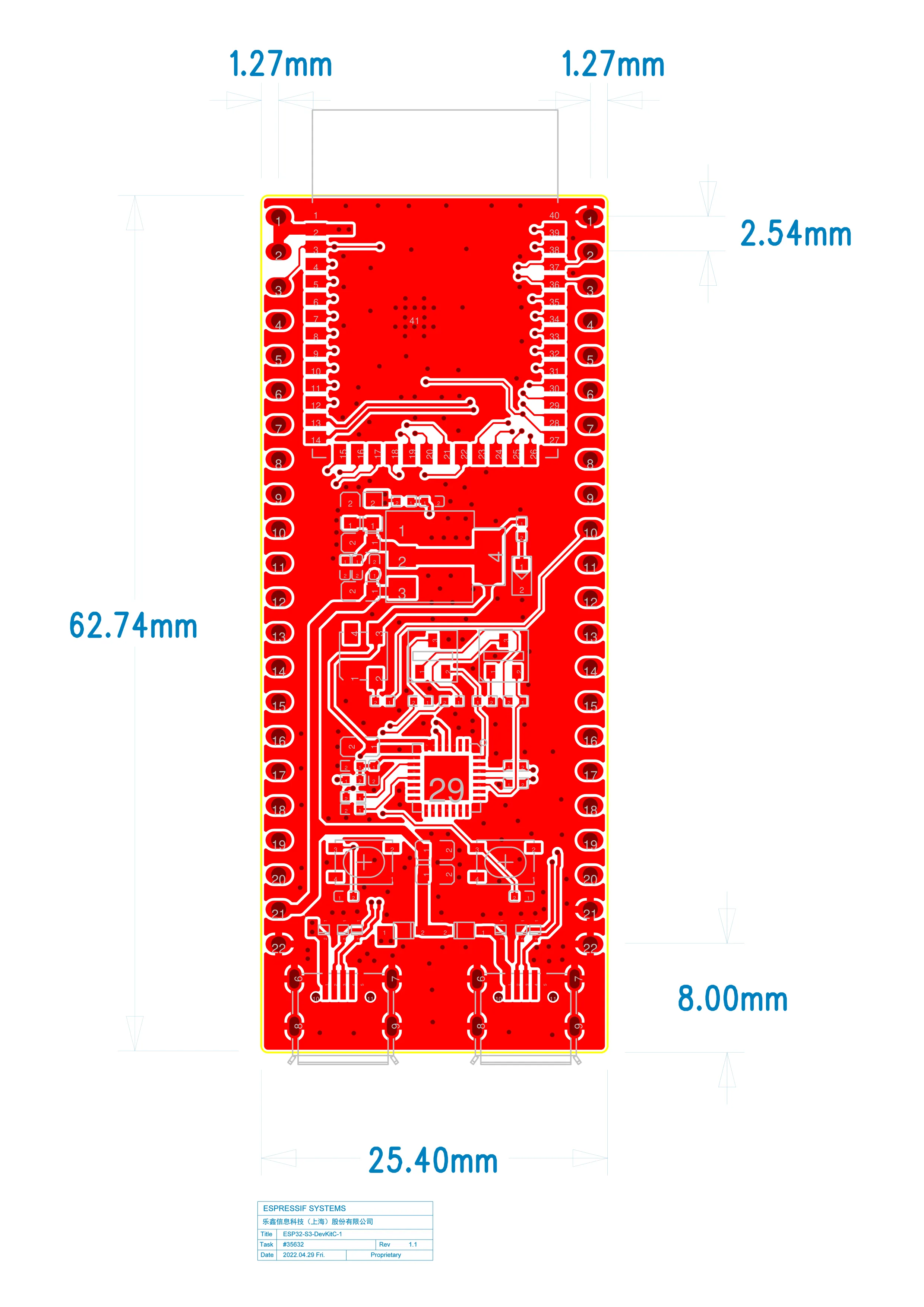
Top Layer
The top layer includes:
- ESP32-S3-WROOM-1 module
- USB connectors (J2, J4)
- CP2102N USB-UART bridge
- Power regulation (U2 LDO)
- User buttons (RST, BOOT)
- RGB LED (D6)
- Header pins (J1, J3)
Key Layout Considerations
- Module Placement: The WROOM module is centered with its antenna extending beyond the board edge
- USB Ports: Placed at opposite ends for cable clearance
- Buttons: Accessible from board edge
- LED: Near GPIO header for visual status
Bottom Layer
The bottom layer contains:
- Ground plane (majority of area)
- Power traces
- Signal routing between headers and module
Pin Legend
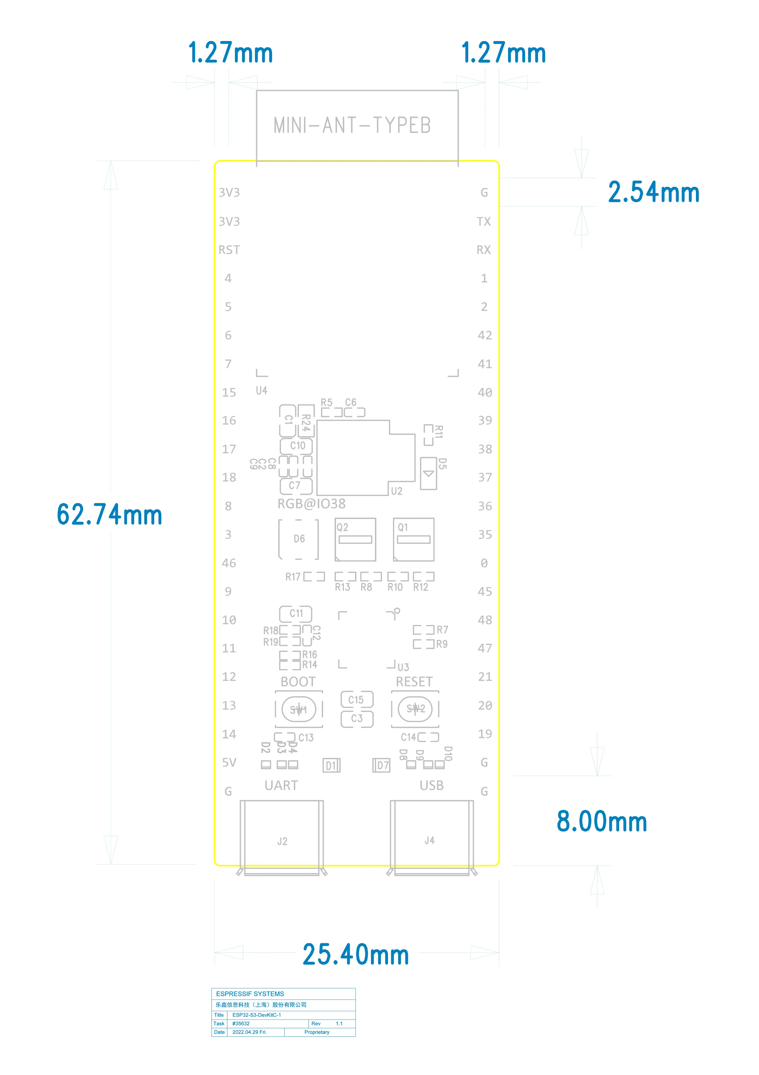
Left Header (J1) - 22 Pins
From USB side down:
3V3 ─ ● 13V3 ─ ● 2RST ─ ● 34 ─ ● 45 ─ ● 56 ─ ● 67 ─ ● 715 ─ ● 816 ─ ● 917 ─ ● 1018 ─ ● 118 ─ ● 123 ─ ● 1346 ─ ● 149 ─ ● 1510 ─ ● 1611 ─ ● 1712 ─ ● 1813 ─ ● 1914 ─ ● 205V ─ ● 21G ─ ● 22Right Header (J3) - 22 Pins
From USB side down:
G ─ ● 1TX ─ ● 2RX ─ ● 31 ─ ● 42 ─ ● 542 ─ ● 641 ─ ● 740 ─ ● 839 ─ ● 938 ─ ● 10 (RGB LED - V1.1)37 ─ ● 11 (PSRAM)36 ─ ● 12 (PSRAM)35 ─ ● 13 (PSRAM)0 ─ ● 14 (Boot)45 ─ ● 1548 ─ ● 16 (RGB LED - V1.0)47 ─ ● 1721 ─ ● 1820 ─ ● 19 (USB D+)19 ─ ● 20 (USB D-)G ─ ● 21G ─ ● 22Component Placement
Active Components
| Ref | Component | Location |
|---|---|---|
| U2 | SGM2212 LDO | Near 5V input |
| U3 | CP2102N | Center, between USB ports |
| U4 | ESP32-S3-WROOM-1 | Top center |
| Q1, Q2 | L8050QLT1G | Near CP2102N |
| D6 | SK68XXMINI-HS | Right edge |
Passive Placement
- Decoupling capacitors placed close to IC power pins
- USB resistors near USB connectors
- Pull-up/down resistors near associated GPIO
Antenna Considerations
The PCB antenna is located at the top edge of the WROOM module:
Best Practices
- Orient module so antenna faces away from noise sources
- Keep antenna edge at enclosure opening if used
- Avoid placing near metal objects or human body contact areas
Mounting
Header Options
| Option | Use Case |
|---|---|
| Male headers (default) | Breadboard insertion |
| Female headers | Stacking, jumper wires |
| No headers | Custom integration |
Mounting Holes
The board does not include mounting holes. For enclosure mounting:
- Use header pins for mechanical support
- Consider 3D-printed brackets
- Use adhesive standoffs
Design Files
For custom designs or manufacturing:
- Schematic: SCH_ESP32-S3-DevKitC-1_V1.1_20221130.pdf
- PCB Layout: PCB_ESP32-S3-DevKitC-1_V1.1_20220429.pdf
- Dimensions: DXF_ESP32-S3-DevKitC-1_V1.1_20220429.dxf
Breadboard Compatibility
The DevKitC-1 fits standard breadboards:
- 2.54mm header pitch matches breadboard
- Board width spans the center gap
- All pins accessible on both sides