Schematic Walkthrough
This page explains the key circuit sections of the ESP32-S3-DevKitC-1 V1.1 schematic.
Block Diagram
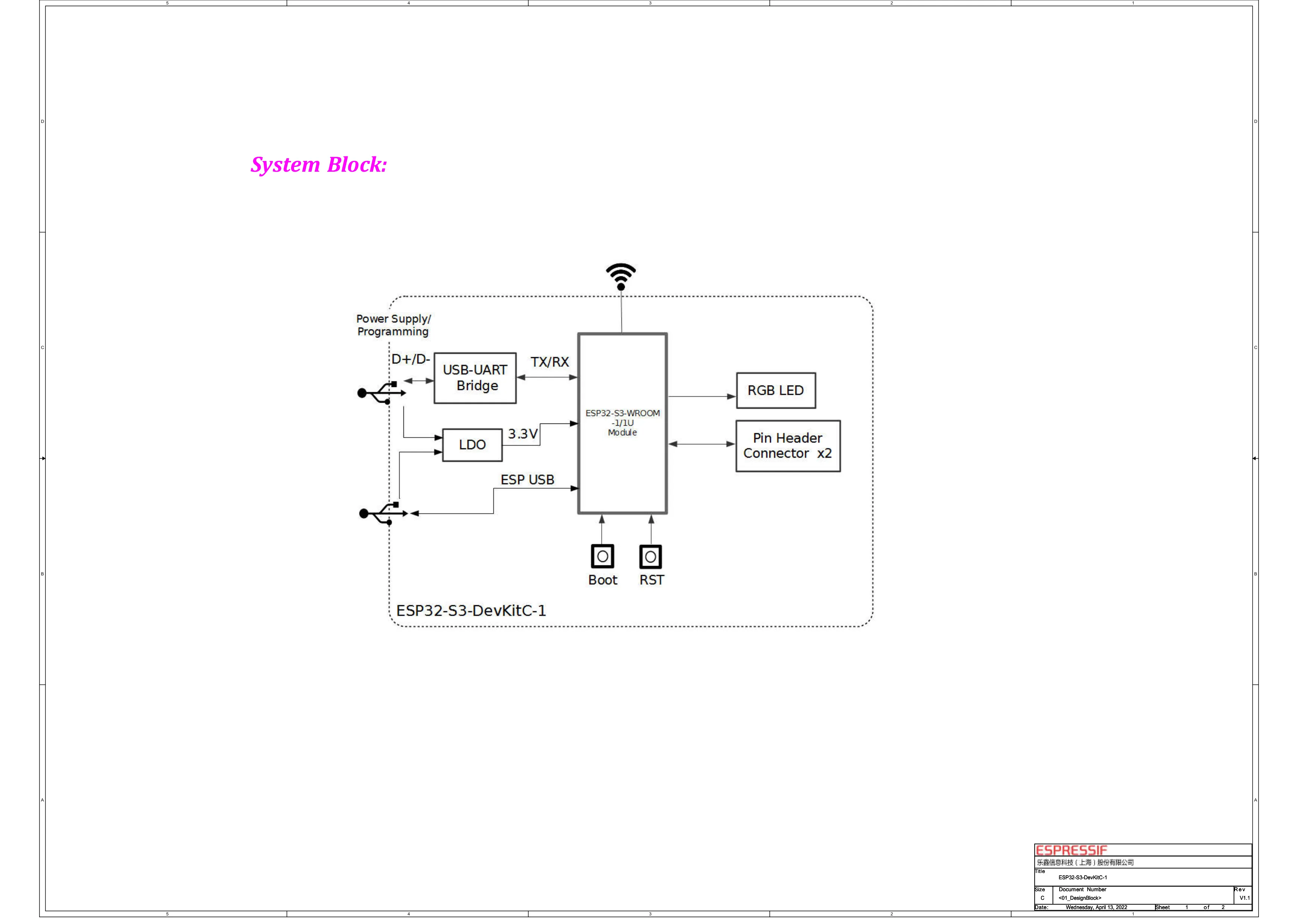
The board consists of five main sections:
- Power Supply - 5V input, 3.3V LDO regulation
- ESP32-S3-WROOM-1 - The main MCU module
- USB-UART Bridge - CP2102N for serial communication
- Auto-Programming - Automatic boot mode selection
- User Interface - RGB LED, buttons
Detailed Schematic
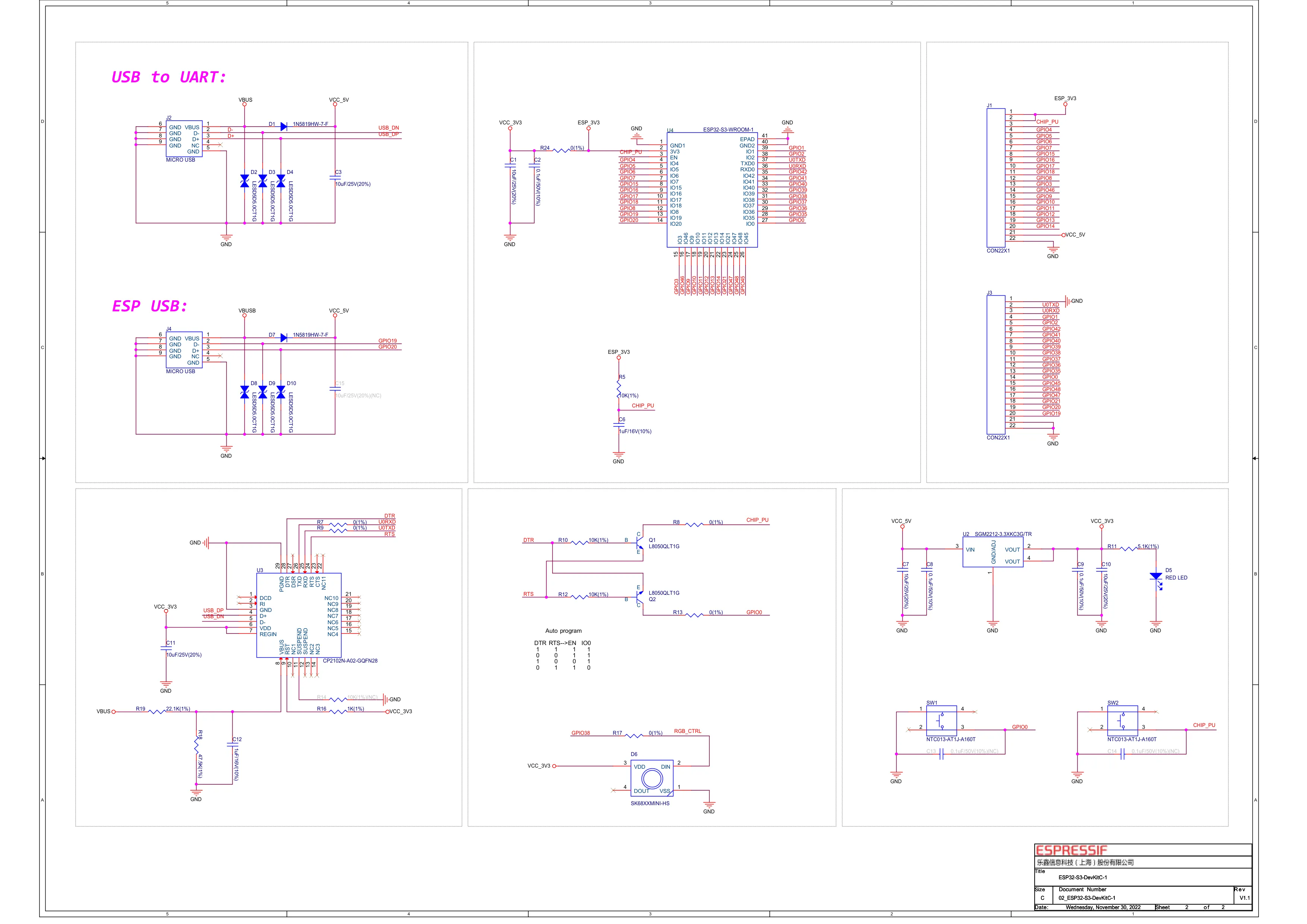
Power Supply Section
Input Protection
graph LR
    USB["USB 5V"] --> D1["D1 (1N5819HW)"]
    EXT["External 5V"] --> D7["D7"]
    D1 --> LDO["To LDO"]
    D7 --> LDO
The Schottky diodes (D1, D7) provide:
- Reverse polarity protection
- OR-ing of multiple power sources
- Low ~0.3V forward drop
Voltage Regulation
| Component | Value | Function |
|---|---|---|
| U2 | SGM2212-3.3 | 3.3V LDO |
| C3, C7 | 10μF | Input/output filtering |
| C2, C8 | 0.1μF | High-frequency decoupling |
The SGM2212 provides stable 3.3V up to 500mA with:
- Wide input range (4.5-5.5V)
- Low dropout (300mV @ 500mA)
- Thermal protection
ESP32-S3-WROOM-1 Module
Module Pinout
The 41-pin module exposes:
| Pin Group | Pins | Notes |
|---|---|---|
| Power | 3V3, GND | Multiple GND pins |
| Reset | EN (CHIP_PU) | Active low reset |
| Boot | GPIO0 | Strapping pin |
| USB | GPIO19, GPIO20 | D-, D+ |
| UART | U0TXD, U0RXD | GPIO43, GPIO44 |
| GPIO | GPIO1-48 | Various functions |
Module Power Pins
| Pin | Connection |
|---|---|
| Pin 2 (3V3) | 3.3V rail |
| Pin 1, 40, 41 | GND |
| VDD_SPI (internal) | 3.3V for flash/PSRAM |
USB-UART Bridge
CP2102N Circuit
graph LR
    DP["USB D+"] --> CP["CP2102N"]
    DM["USB D-"] --> CP
    V5["5V"] --> CP
    GND --> CP
    CP --> TXD["U0TXD (GPIO44)"]
    RXD["U0RXD (GPIO43)"] --> CP
    CP --> DTR
    CP --> RTS
Key Connections
| CP2102N Pin | Connection | Function |
|---|---|---|
| VDD | 3.3V | Logic power |
| VREGIN | 5V USB | Regulator input |
| D+/D- | USB | USB data |
| TXD | U0RXD | Serial TX → ESP RX |
| RXD | U0TXD | Serial RX ← ESP TX |
| DTR | Auto-program | Data Terminal Ready |
| RTS | Auto-program | Request to Send |
ESD Protection
USB data lines are protected by LESD5D5.0CT1G TVS diodes:
- Clamp voltage: 5V
- Peak pulse current: 15A
- Low capacitance: 0.5pF
Auto-Programming Circuit
This circuit allows automatic entry into download mode without pressing buttons.
Circuit Operation
graph TD
    DTR --> Q1["Q1 (NPN)"]
    RTS --> Q2["Q2 (NPN)"]
    Q1 --> EN
    Q2 --> GPIO0
    Q1 -.->|"cross-coupled"| Q2
    Q2 -.->|"cross-coupled"| Q1
Logic Table
| DTR | RTS | EN | GPIO0 | Mode |
|---|---|---|---|---|
| 1 | 1 | 1 | 1 | Normal run |
| 0 | 0 | 1 | 1 | Normal run |
| 1 | 0 | 0 | 1 | Reset |
| 0 | 1 | 1 | 0 | Download mode |
Transistors (Q1, Q2)
L8050QLT1G NPN transistors with:
- 10K base resistors (R5, R10)
- Cross-coupled for proper sequencing
User Interface
RGB LED (D6)
| Component | Value | Function |
|---|---|---|
| D6 | SK68XXMINI-HS | Addressable RGB |
| R16 | 1K | Data line resistor |
| GPIO | 38 (V1.1) | Control signal |
The SK68XXMINI-HS is WS2812-compatible:
- Single-wire protocol (800 kHz)
- 24-bit color (8-bit per channel)
- Internal 5V to 3.3V level shifter
Power LED (D5)
| Component | Value |
|---|---|
| D5 | Red LED |
| R (series) | ~1K |
| Connection | 3.3V rail |
Always illuminated when power is applied.
Buttons
| Button | GPIO | Function | Pull-up |
|---|---|---|---|
| RST (SW1) | CHIP_PU (EN) | System reset | External 10K |
| BOOT (SW2) | GPIO0 | Boot strapping | Internal |
Button part: NTC013-AT1J-A160T (4-pad SMD)
Native USB Connection
ESP32-S3 USB-OTG
graph LR
    DP["USB (J2) D+"] --> D8["TVS (D8)"] --> GPIO20
    DM["USB (J2) D-"] --> D9["TVS (D9)"] --> GPIO19
    VBUS["USB (J2) VBUS"] --> D7 --> RAIL["5V Rail"]
    ID["USB (J2) ID"] --> R11["R11 (5.1K)"] --> GND
- R11 (5.1K, 1%) is a USB CC/ID pull-down resistor for device mode identification
- D8, D9 (LESD5D5.0CT1G) provide ESD protection on D+/D-
- No series resistors on the data lines — the ESP32-S3 internal USB PHY handles signaling directly
- The ESP32-S3 uses a Synopsys DesignWare Core (DWC2) USB 2.0 OTG controller with integrated transceiver
USB Power Delivery
| Pin | Connection |
|---|---|
| VBUS | 5V via D7 (Schottky) |
| GND | Common ground |
| ID | Not connected (device mode) |
USB OTG Host Jumper (Unpopulated)
By default, VBUS power flows into the board: USB host → D7 (Schottky) → 5V rail. The diode blocks reverse current, so the board cannot supply 5V to connected USB devices.
Device mode (default):
graph LR
    HOST["USB Host 5V"] -->|"power IN"| D7["D7 (Schottky)"] --> RAIL["5V Rail"]
    RAIL2["5V Rail"] -.-x|"blocked by diode"| VBUS
Host mode (OTG jumper soldered):
graph LR
    RAIL["5V Rail"] -->|"power OUT"| J["0Ω Jumper"] --> VBUS
To enable USB OTG host mode:
- Solder a 0Ω resistor (or solder bridge) across the “USB OTG” pads
- Power the board externally (not through J2) to avoid VBUS conflicts between two 5V sources
- Use ESP-IDF’s
usb_host_install()driver — see the USB Host tutorial
Passive Components
Capacitors
| Designator | Value | Type | Notes |
|---|---|---|---|
| C1, C3, C7, C10, C11 | 10μF | Ceramic | Bulk filtering |
| C2, C8, C9 | 0.1μF | Ceramic | Decoupling |
| C6, C12 | 1μF | Ceramic | USB filtering |
Resistors
| Function | Value | Designators |
|---|---|---|
| Pull-up/down | 10K | R5, R10, R12 |
| USB ID pull-down | 5.1K | R11 |
| LED current | 1K | R16 |
| Voltage divider | 47.5K/22.1K | R18, R19 |
| Jumpers | 0Ω | R7, R8, R9 |
Design Notes
Ground Planes
- Continuous ground pour on bottom layer
- Via stitching around RF section
- Separate analog/digital grounding near ADC
Antenna Clearance
Keep the area around the PCB antenna free of:
- Metal components
- Ground planes
- High-frequency traces